Overview
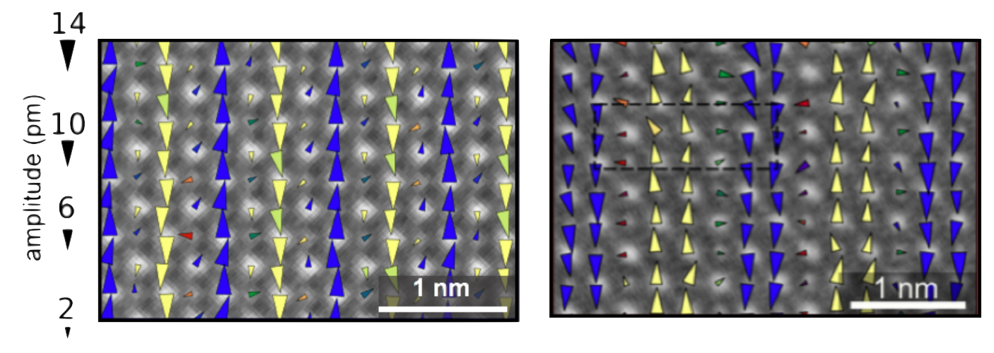
Atomic-resolution cryogenic electron microscopy of low temperature trimers in a 2D material
Strongly correlated electronic materials host a myriad of fascinating structural, electronic and magnetic ground states as well as complex behaviors ranging from the nanoscale coexistence of competing phases to a huge sensitivity to external stimuli. Our laboratory utilizes in situ electron microscopy to visualize and manipulate these materials at the atomic scale.
Techniques
The instrument at the heart of our research is the scanning transmission electron microscope (STEM) which provides vivid atomic-resolution images of crystalline materials. To access and manipulate the rich phases of strongly correlated materials, both ultra-stable cryogenic sample holders and in situ control knobs are essential.
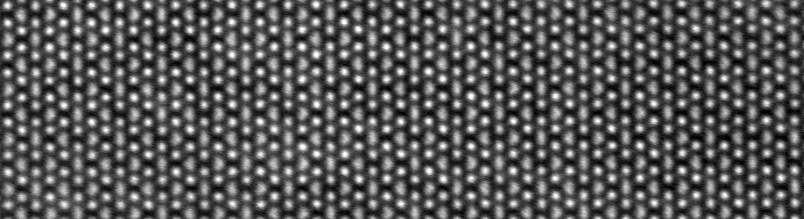
The advent of high-resolution cryogenic STEM imaging near 90 K has enabled unprecedented microscopic insights, such as the direct visualization of the picometer scale distortions that accompany charge and orbital order, topological defects in stripes, and trimerization in a 2D material.
Picometer-scale atomic displacements in the charge order phase of manganites
Recently, we have developed a novel instrument that enables cooling using liquid helium. The low-vibration design enables atomic-resolution imaging and stable temperature performance. A broad range of electronic, optical and quantum phases are now accessible to electron microscopy. .
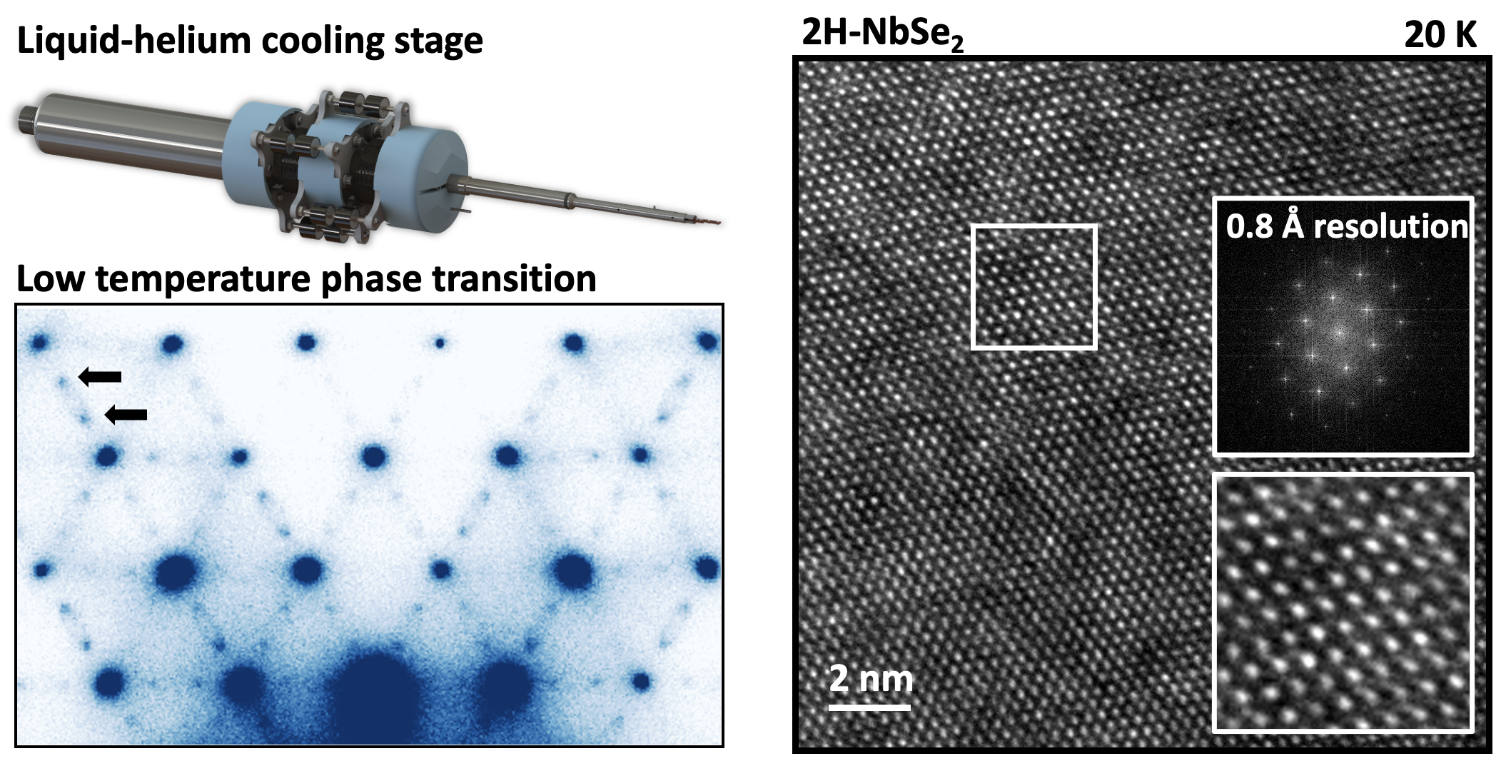
Liquid helium stage for probing materials at low temperature in the scanning transmission electron microscope
Topics
The materials we study range from bulk complex oxides to atomically engineered heterointerfaces to quasi-2D and quasi-1D compounds. These systems provide a rich playground for studying phenomena such as charge and orbital order, superconductivity, phase separation, ferroelectricity and quantum criticality.
We are interested in understanding phase transitions by directly visualizing order and disorder. Examples include real space observations of topological defects in charge-ordered stripes, atomic-scale tracking of charge order dislocations across temperatures, and discovering an inverse transition in a chemically doped ferroelectric.